
Photoabsorption Imaging at Nanometer Scales Using Secondary Electron Analysis
 Nano Lett. 2021, 21, 5, 1935–1942
Ze Zhang, Joel Martis, Xintong Xu, Hao-Kun Li, Chenlu Xie, Brad Takasuka, Jonghoon Lee, Ajit K. Roy, and Arun Majumdar
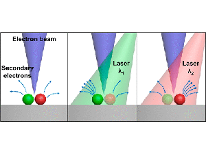
The abstract reads as follows: Optical imaging with nanometer resolution offers fundamental insights into light–matter interactions. Traditional optical techniques are diffraction limited with a spatial resolution >100 nm. Optical super-resolution and cathodoluminescence techniques have higher spatial resolutions, but these approaches require the sample to fluoresce, which many materials lack. Here, we introduce photoabsorption microscopy using electron analysis, which involves spectrally specific photoabsorption that is locally probed using a scanning electron microscope, whereby a photoabsorption-induced surface photovoltage modulates the secondary electron emission. We demonstrate spectrally specific photoabsorption imaging with sub-20 nm spatial resolution using silicon, germanium, and gold nanoparticles. Theoretical analysis and Monte Carlo simulations are used to explain the basic trends of the photoabsorption-induced secondary electron signal. Based on our current experiments and this analysis, we expect that the spatial resolution can be further improved to a few nanometers, thereby offering a general approach for nanometer-scale optical spectroscopic imaging and material characterization.
This work was supported as part of the Center for Enhanced Nanofluidic Transport, an Energy Frontier Research Center funded by the U.S. Department of Energy, Office of Science, Basic Energy Sciences under Award # DE-SC0019112.
https://pubs.acs.org/doi/10.1021/acs.nanolett.0c03993